Get Smart
With its expertise in CMP polishing as well as in-situ cleaning, EBARA has investigated and developed early on equipment and process solutions to help customers solving their edge problems by “conditioning” the bevel. EBARA’s bevel polishing systems employ novel polishing techniques to process the bevel and backside of the wafers – an area that has attracted attention in recent years as a source of defects amid efforts to improve the yield rate of semiconductor production.
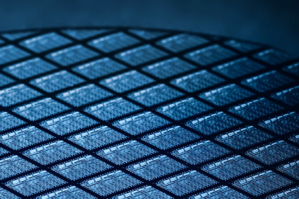
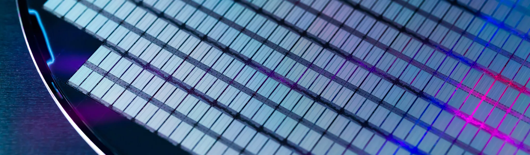
Bevel Polishing: Clean and Reshape Wafer
As the main source for wafer yield loss, our bevel polishing tools not only remove damages
to the wafer edge, but also clean and reshape the bevel.
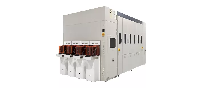
For high volume production fully automated systems – EAC200bi-hp / EAC300bi-hv
Core Benefits

Applications with EAC Tools
- Removal of any films even SI
- Clean and reshape bevels
- Mechanical polishing on bevel area
- Mechanical polishing on top edge area
- Mechanical polishing on notch area
- Physical polish with high effective touch-ups
- Accurate polishing profile control
- Trench etching
- Power device maker