Enhanced Mask Plating
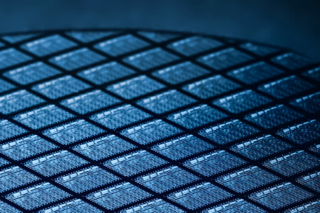
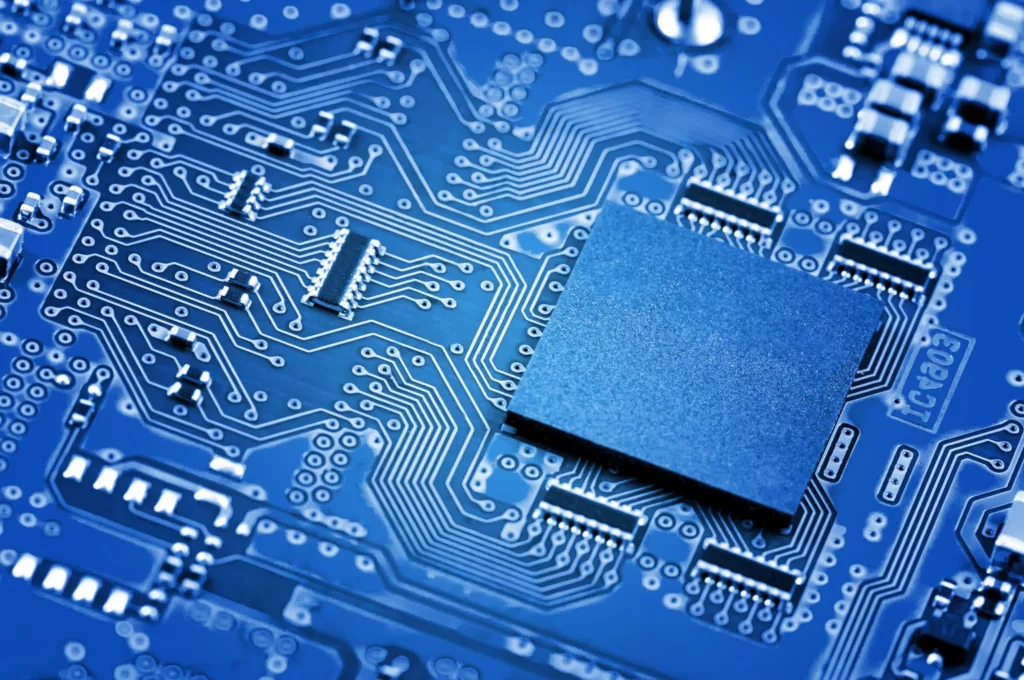
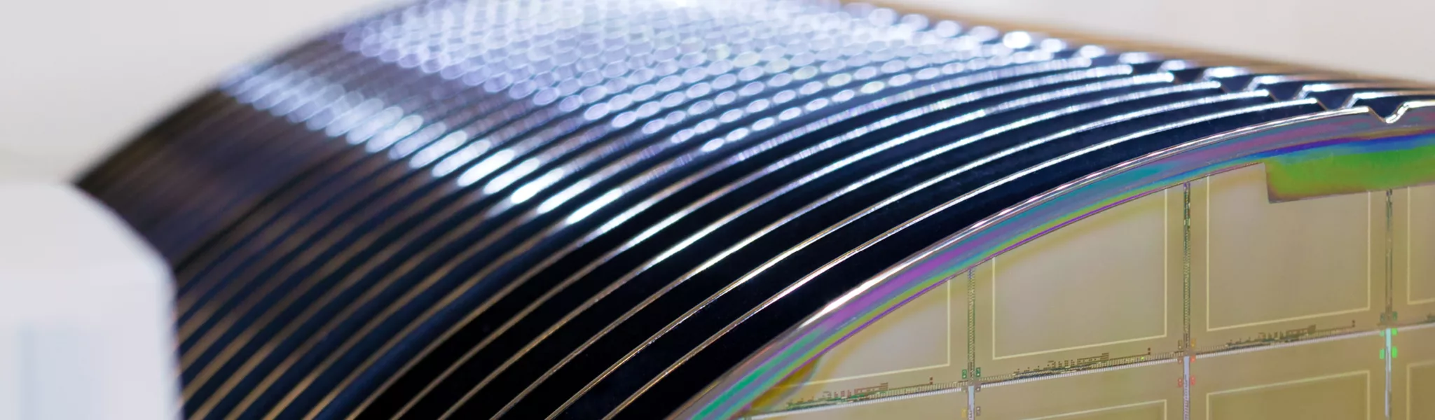
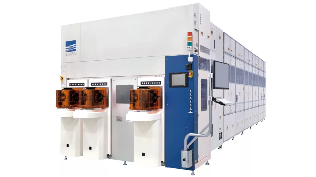
The wafer plating systems enable fast, high performance processing for depositing fine conductive patterns on wafers. This includes bumps, pillars, re-wirings and through silicon via structures, which are essential for packaging techniques.
Core Benefits

Applications for UFP Models
- Redistribution
- Bumping
- IC Advanced Packaging
- Wafer Level Chip Packaging
- Multi-layer Applications
- Patterned Plating (Copper, Nickel, Gold, Solder)