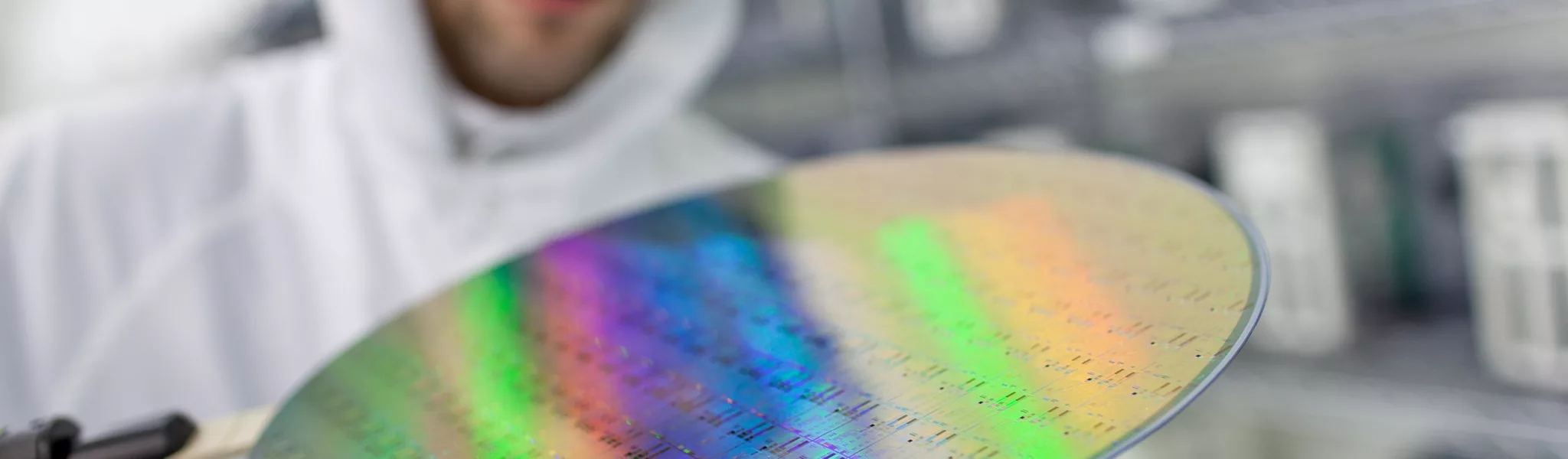
One Step Ahead
EBARA products and system solutions drive the evolution of the semiconductor industry with high-precision manufacturing technologies. From smartphones, tablets and Internet of Things (IoT) to infrastructure devices such as cloud servers, EBARA manufactures the excellent precision tools and machinery that help build these devices. Over 80% of the top 20 chip manufacturers are EBARA customers.
Core Benefits
Learn more about our Systems.

Applications for the Semiconductor Manufacturer
- Lithography-Metrology
- Surface Analysis
- Physical Vapor Deposition (PVD)
- Atomic Layer Deposition (ALD)
- Chemical Vapor Deposition (CVD)
- Rapid Thermal Processing (RTP)
- Silicium Technology
- Ashing
- Sputtering
- Ion Implant
- Diffusion
- Residual Gas Analysis
- Epitaxy
- Load Lock Vacuum
- Micro Machining (MEMS)
Systems for Semiconductor Manufacturers
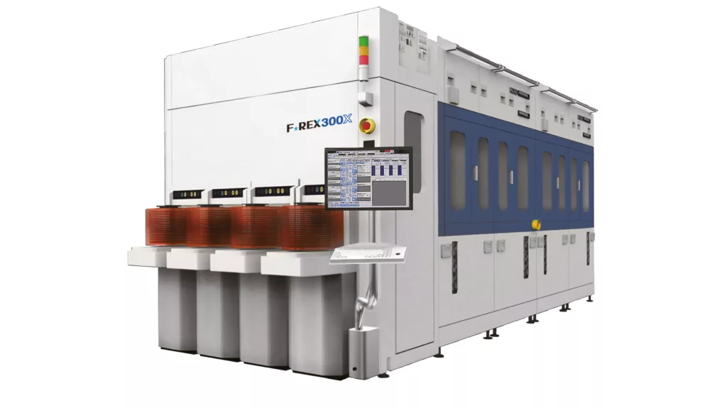
We provide the semiconductor industry with the best suited solutions using vacuum technology
with dry vacuum pumps, gas abatement and CMP Systems.